User manual CADENCE DESIGN SYSTEMS 3D DESIGN VIEWER DATASHEET
Lastmanuals offers a socially driven service of sharing, storing and searching manuals related to use of hardware and software : user guide, owner's manual, quick start guide, technical datasheets... DON'T FORGET : ALWAYS READ THE USER GUIDE BEFORE BUYING !!!
If this document matches the user guide, instructions manual or user manual, feature sets, schematics you are looking for, download it now. Lastmanuals provides you a fast and easy access to the user manual CADENCE DESIGN SYSTEMS 3D DESIGN VIEWER. We hope that this CADENCE DESIGN SYSTEMS 3D DESIGN VIEWER user guide will be useful to you.
Lastmanuals help download the user guide CADENCE DESIGN SYSTEMS 3D DESIGN VIEWER.
Manual abstract: user guide CADENCE DESIGN SYSTEMS 3D DESIGN VIEWERDATASHEET
Detailed instructions for use are in the User's Guide.
[. . . ] CAD E N C E 3 D D E S I G N V I E W E R
VISU A L I Z E , D E B U G , A N D V E R I F Y COM P L E X I C PA C K A G E S
DATASHEET
AN INTELLIGENT 3D DESIGN VIEW
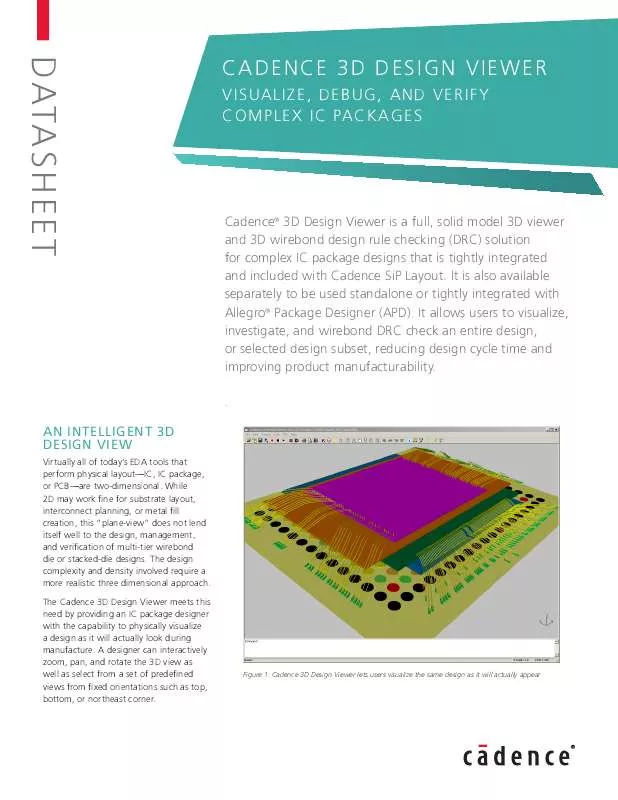
Virtually all of today's EDA tools that perform physical layout--IC, IC package, or PCB--are two-dimensional. While 2D may work fine for substrate layout, interconnect planning, or metal fill creation, this "plane-view" does not lend itself well to the design, management, and verification of multi-tier wirebond die or stacked-die designs. The design complexity and density involved require a more realistic three dimensional approach. [. . . ] The base die is flip-chip attached; the top three die are wirebond attached. In the 2D editor view (Figure 2), visualizing and validating the die stack and the wirebond ring is challenging, even for a seasoned package designer. And, due to the complexity, it would be almost impossible to hold a design review with an architect or lead engineer. When the same design is loaded into the 3D Design Viewer (Figure 1) the designer and the engineering team can not only easily visualize, investigate, and create collaborative. markups but they can also perform detailed 3D wirebond checking, including the ability to define, modify, and assign new wirebond profiles.
Figure 2: A multi-die stack on a BGA substrate viewed in 2D
the highlight color and the level of transparency applied to none selected objects. The 3D Viewer is especially effective when trying to understand and visualize complex via arrays, especially on designs using build-up layers. Figure 3 illustrates how difficult it is to understand the
connectivity path of high density interconnect (HDI) from a top package substrate layer to a bottom layer viewed in 2D. Contrast this figure with the 3D view of the same HDI. The designer can easily visualize the interconnect path from the top to the bottom layer.
EASY DESIGN INVESTIGATION
Cross referencing is easy as the 3D Design Viewer uses the same color/layer/object settings as defined in Allegro Package Designer. Layer visualization can be turned on/off and layer transparency set. For detailed design investigation, the 3D Viewer has similar "show element" information command capability that can be used by "object" or by "net. " Importantly, the user has control over
Figure 3: It is difficult to understand the connectivity path between the metal interconnect as it transitions between layers in 2D
www. cadence. com
3D DESIGN VIEWER
2
ADVANCED FEATURES
When preparing for 3D viewing in SiP Layout or APD, it may be desirable to focus on a sub-section of the package. For this reason, the user is offered the option of taking a section of the package and viewing that piece in the 3D viewer. This can be particularly useful in design reviews where a section of the design is being examined. Another useful feature is the ability to append multiple designs within one single 3D view. [. . . ] Because the 3D Design Viewer leverages wire curvature
Figure 5: Cadence 3D Design Viewer allows for detailed study of sections of a design to be sectioned out and visualized in 3D.
www. cadence. com
3D DESIGN VIEWER
3
Figure 6 shows how the 3D Viewer enhances the designers debug capability--the "info" command highlights the DRC marker and the associated wirebonds as well as indicating the rule, rule value, and actual value.
CADENCE SERVICES AND SUPPORT
· Cadenceapplicationengineerscan answer your technical questions by telephone, email, or Internet--they can also provide technical assistance and custom training · Cadencecertifiedinstructorsteach more than 70 courses and bring their real-world experience into the classroom · Morethan25InternetLearningSeries (iLS) online courses allow you the flexibility of training at your own computer via the Internet ·CadenceOnlineSupportgivesyou 24x7 online access to a knowledgebase of the latest solutions, technical documentation, software downloads, and more
Figure 6: A design rule violation is highlighted using the info command. 3D visualization lets you see precisely where 3D spacing rules are violated.
For more information contact Cadence sales at:
+1. 408. 943. 1234
or log on to:
www. cadence. com/ contact_us
© 2010 Cadence Design Systems, Inc. Cadence, the Cadence logo, and Allegro are registered trademarks of Cadence Design Systems, Inc. [. . . ]
DISCLAIMER TO DOWNLOAD THE USER GUIDE CADENCE DESIGN SYSTEMS 3D DESIGN VIEWER Lastmanuals offers a socially driven service of sharing, storing and searching manuals related to use of hardware and software : user guide, owner's manual, quick start guide, technical datasheets...manual CADENCE DESIGN SYSTEMS 3D DESIGN VIEWER


